
NanoPulse, Inc., executes agreement with "Kutsari", Mexico’s national semiconductor initiative
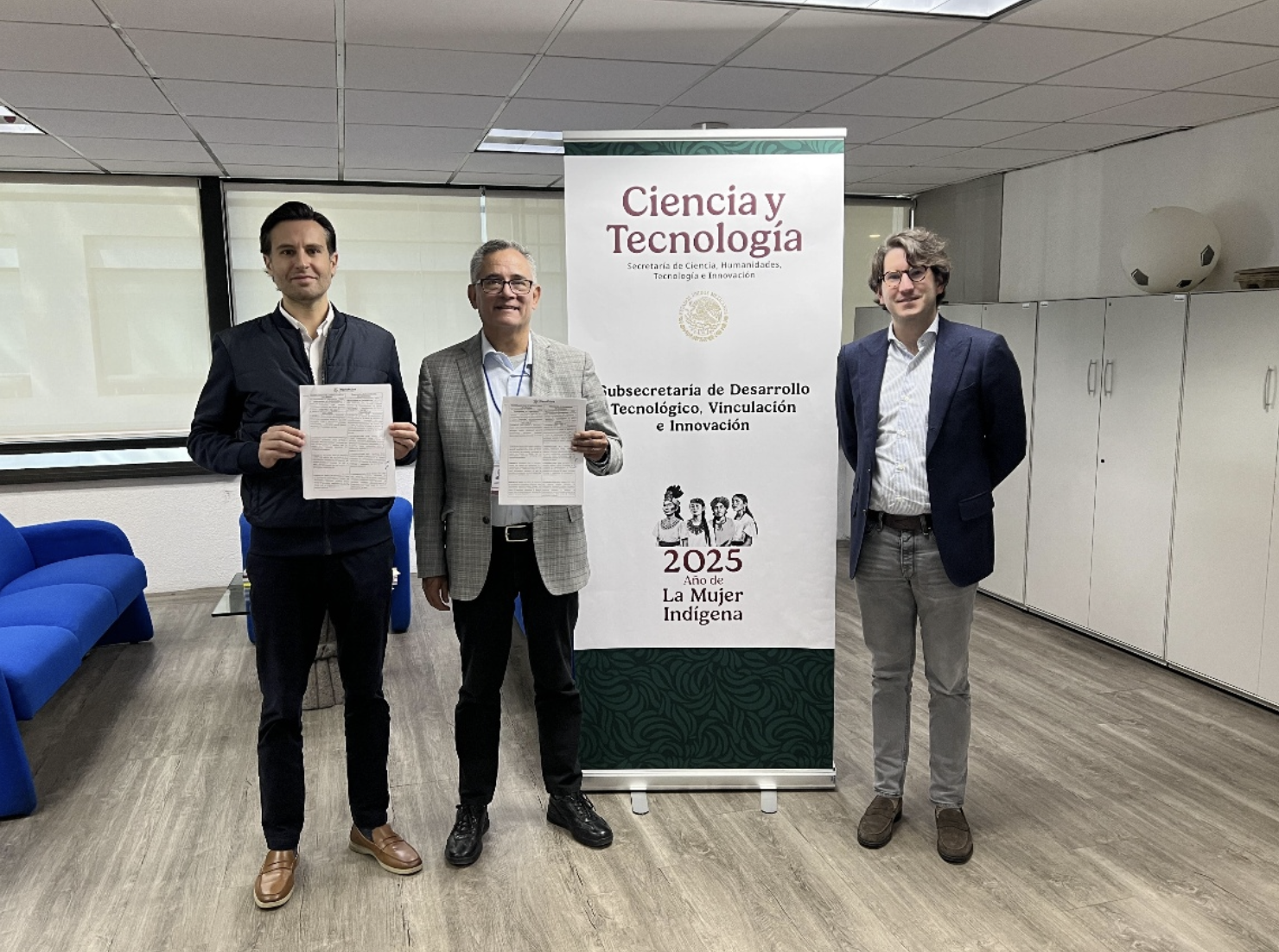
Mexico City – January 27, 2026. NanoPulse, Inc., announced today the execution of an agreement with InnovaBienestar de México S.A.P.I. de C.V., in coordination with the national semiconductor initiative known as “Kutsari”. The collaboration reflects a shared commitment to strengthening Mexico’s role in North America’s semiconductor supply-chain realignment through advanced packaging, design, talent development, and applied innovation.
Under the agreement, the parties intend to collaborate on workforce development, curriculum modernization, research and development initiatives, and joint outreach efforts aligned with industry needs. The framework emphasizes visibility, strategic cooperation, and ecosystem building, while enabling flexibility for future, project-specific agreements. The initiative is designed to help accelerate the development of a robust semiconductor talent pipeline and reinforce Mexico’s competitiveness as a nearshoring destination.
“This collaboration is about signaling ambition and building the foundations of a world-class semiconductor ecosystem in Mexico,” said Marcelo de Antuñano, CEO and Co-Founder of NanoPulse. “By aligning with Kutsari/InnovaBienestar, we are reinforcing our commitment to talent, technology, and long-term industrial capacity that supports North American supply-chain resilience.”
About NanoPulse, Inc.
NanoPulse is an American company with operations in Mexicali, Mexico founded by private equity professionals with extensive cross-border transactional experience, in partnership with senior U.S. Assembly, Test and Packaging and Design experts who each brings decades of leadership from top-tier semiconductor companies.
Amid growing concerns over national security, nearshoring trends, increased semiconductor demand, and strong manufacturing tailwinds, NanoPulse serves the specialized needs of North American semiconductor clients and other industry players from the automotive, telecom, aerospace, manufacturing, healthcare, robotics, and electronics industries.
North American–fabricated wafers will command a premium. By locating advanced packaging and testing in Mexico, we aim to preserve that premium without increasing overall system costs. Operating in the same time zone, with no tariffs under USMCA, a deep and cost-competitive engineering talent pool, and strong government support on both sides of the border, we eliminate the need to ship wafers to Asia while maintaining costs comparable to Southeast Asia.
We believe investment in North American semiconductor and energy infrastructure is a winning trade immediately, and increasingly so over the next 1, 5, and 10 years as the region builds a resilient, reliable, and geographically proximate supply chain.
Website: www.nanopulse.co
Media inquiries: info@nanopulse.co